


Tata Electronics hires top experts to put Dholera fab on a firmer footing
Tata Electronics has engaged global engineering experts to redesign the foundation of its semiconductor fab at Dholera, ensuring stability and adherence to strict technical standards.
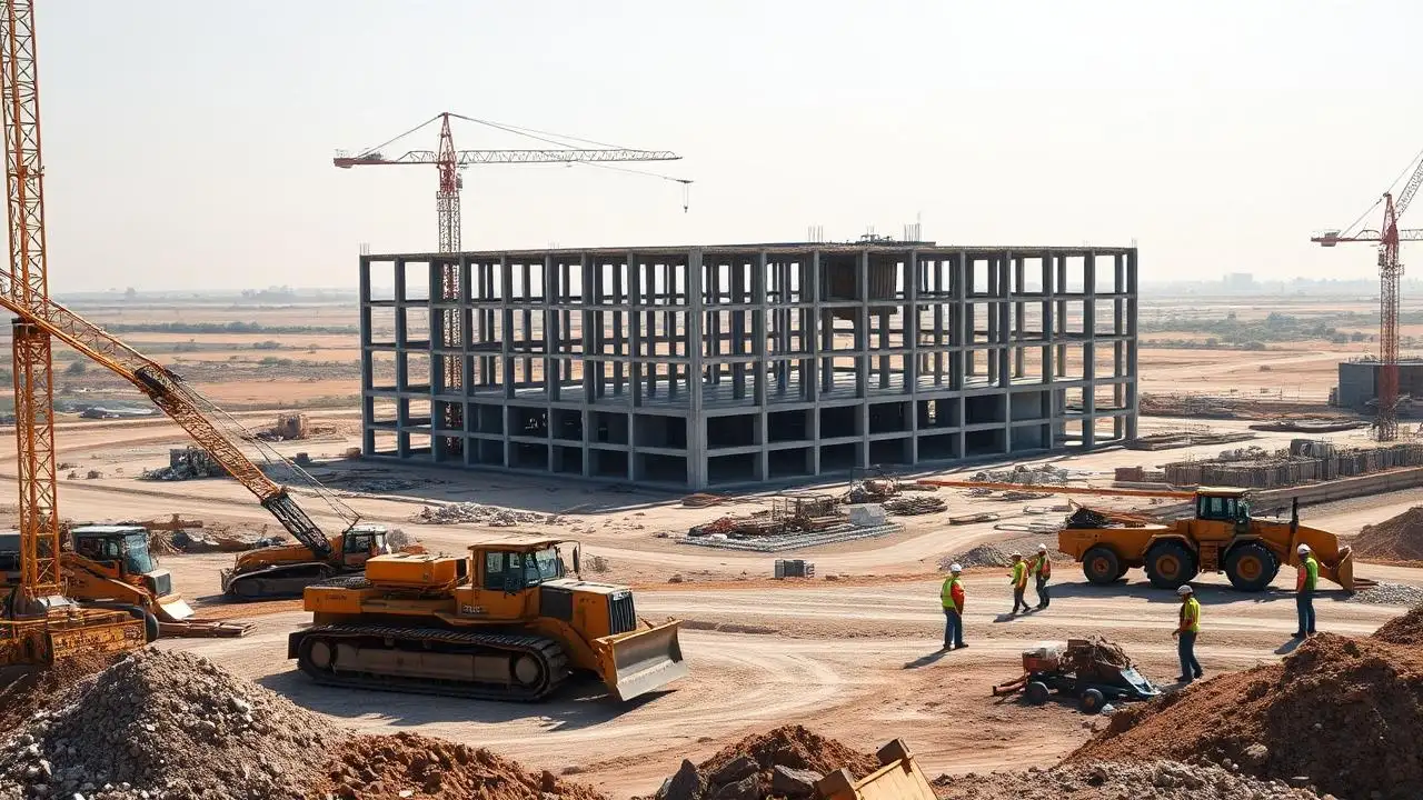
Tata Electronics has initiated a major redesign of the foundations for its upcoming semiconductor fabrication plant in Dholera, Gujarat, after site assessments revealed complex soil conditions. The Rs 91,000-crore project, being built in partnership with Taiwan’s PSMC and scheduled to start chip production by December 2026, is situated on reclaimed land with challenging geology.
According to sources, the soil is clay-heavy, saline, silty, and has low load-bearing capacity. Semiconductor fabs require stringent specifications for vibration and weight distribution, making the foundation critical to long-term stability.
To address this, Tata Electronics engaged global geo-data specialist Fugro and geotechnical engineering consulting firm Cengers. The experts conducted detailed geological tests and recommended a revised foundation design tailored to the technical demands of chip manufacturing. Construction of the core fab building has resumed at full pace, while earlier groundwork will now be repurposed for support structures such as utility blocks and warehouses.
A company spokesperson said, "Given the unique geotechnical conditions of the region, we have prioritised rigorous planning and engaged world-class experts to implement comprehensive design and engineering solutions." The company confirmed that, despite the redesign, the project timeline remains on track.
 Whatsapp